For the first time a team of researchers from FOM Institute AMOLF have synthesized a mineral (AgFeS2) to create semiconducting nanowires. This earth-abundant semiconductor has a direct band gap of 0.88 eV and thus could form the basis for a cheap bottom cell in a multi-junction photovoltaic material. This work was published in the Journal of the American Chemical Society on March 26, 2015.
The best of two worlds
The discovery and development of novel nanomaterials is an important cornerstone of research in optoelectronic devices. Device performance depends strongly on the properties of the semiconductor materials employed. A big effort is ongoing to find suitable materials with excellent properties that can be obtained at low costs via solution processing. On the other hand, semiconductor nanowires have proven effective in boosting light absorption via optical resonances that can be tuned according to their size.
Researchers at AMOLF, combining these two worlds have developed a solution-process route to obtain nanowires of the ternary semiconductor AgFeS2. The study shows that such AgFeS2 nanowires can be obtained by reacting Ag nanowires with Fe and S precursors. The researchers showed that the chemical conversion takes place through an intermediate step, where Ag2S is formed. They also showed that by adjusting the reaction temperature, nanotubes could be obtained. This novel nanomaterial was characterized with several techniques (SEM, TEM, XRD, UV-Vis) and showed a direct band gap of 0.88 eV.
Other applications
This study suggests that this process can be extended to other ternary materials, and that the morphology can be controlled by choosing the appropriate metallic nanostructure precursor. This opens the door to appealing applications based on this novel nanomaterial, but also paves the way for material scientists to develop new nanostructures.
Reference
Beniamino Sciacca, Anil O. Yalcin, and Erik C. Garnett, Transformation of Ag Nanowires into Semiconducting AgFeS2 Nanowires J. Amer. Chem. Soc. 137, 4340-4343 (2015) | DOI: 10.1021/jacs.5b02051
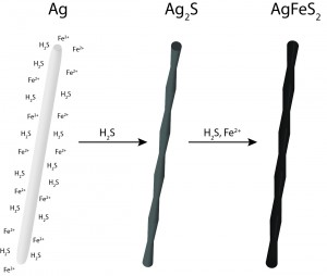
Transformation of silver to semiconductor AgFeS2