Open Technology Programme (OTP) funding

Crystal structure of the perovskite material. Source: AMOLF In the Open Technology Programme (OTP) call for proposals of NWO, Bruno Ehrler and Erik Garnett have received…

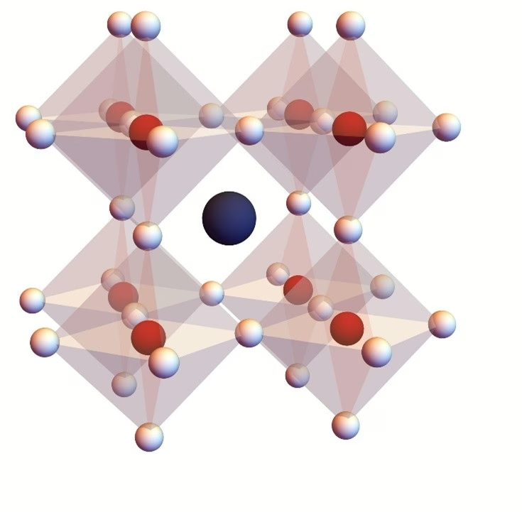
Crystal structure of the perovskite material. Source: AMOLF

In the Open Technology Programme (OTP) call for proposals of NWO, Bruno Ehrler and Erik Garnett have received funding to carry out the research plan ‘Achieving Semiconductor Stability from the Ground Up’. The OTP call for proposals is open to excellent research aimed at the possible implementation of the results. In addition to the scientific contribution carried out by AMOLF, the following companies are involved: EDAX (subsidiary of Ametek), CL Solutions (part of Delmic), and Amsterdam Scientific Instruments (ASI). The total project receives 1.1 million euros.

Research plan
Halide perovskites have emerged as the most exciting new semiconductor for optoelectronic devices (solar cells, LEDs, radiation detectors) over the last decade. Their performance matches or exceeds that of traditional semiconductors, but their relatively poor stability under a wide variety of stresses (chemical, electrical, light, heat) is limiting their commercialization. We will develop a new characterization tool that allows us to watch how halide perovskites change under light or electrical bias with nanometer spatial resolution. With this understanding we will control the halide perovskite (in)stability either to eliminate degradation or make programmable materials that can be trained to reconfigure their properties according to the desired output.
Read more about OTP calls
Share article
What's happening

Most recent news items

All news items

Adding a scientific flavor to Zwarte Cross

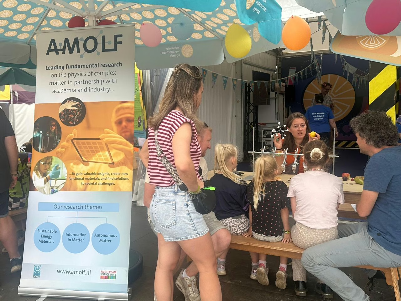
For the first time, AMOLF participated in the Netherlands' largest summer festival, Zwarte Cross. Together with volunteers from NWO, the AMOLF team introduced children to the fascinating world of molecules.…

Read news item

Atom-thin materials: handle with care… and cling film

As materials become thinner – now reaching a thickness of single atoms – it has become ever more difficult to create large enough sheets of these materials and transfer them without cracking them into tiny flakes. Recent work by a broad Amsterdam-based team of scientists, published in the journal ACS Nano, presents a new technique that solves this problem – using an unexpected material that can be found in any home kitchen.

Read news item

Two Veni grants awarded for projects on immune system activation and twisted perovskites

Two researchers have been awarded Veni grants from the Dutch Research Council (NWO) for three-year postdoctoral research projects at AMOLF. Dr. Megan Farrell will conduct her project on how immune…

Read news item
Mechanical-material-that-can-store-move-and-process-information
Stay informed

Get the latest research highlights, events, and news from our institute delivered to your inbox