An international team of scientists has investigated a new type of charge carrier-selective contact for nanowire solar cells based on the surface-gate effect. Those contacts make use of an effect that is ubiquitous in every computer chip. In a field-effect transistor, a surface gate modulates the conductivity of the underlying semiconductor, allowing control over the current flow between the source and drain terminals. Now, the scientists are able to translate this concept to nanowire solar cells by making use of a surface layer to control the conductivity of the nanowire next to a metal point contact. The researchers from AMOLF, the University of Oregon, Eindhoven University of Technology and Delft University of Technology published their results on August 14th, 2018 in the journal Nature Communications.
“Today, semiconductors are at the heart of the computer, lighting and solar energy industry. Even though aimed at completely different applications, fundamentally, transistors and photovoltaics have a key challenge in common: controlling the flow of electronic charge carriers inside a semiconductor”, says Sebastian Oener, a former PhD student in the Nanoscale Solar Cells group at AMOLF and now a postdoctoral researcher at the University of Oregon.
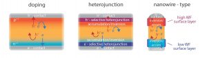
The researchers at AMOLF and their collaborators demonstrate that the nanowire geometry allows them to translate the surface-gate approach from transistors to nanowires. By utilizing a permanent surface layer of another material on top of the nanowire next to the electrode terminal, they modulate the conductivity of the underlying nanowire segment.
Impurity doping
Applying the surface gate approach to nanowire solar cells has several benefits. First, challenges associated with traditional impurity doping at the nanoscale can be mitigated if not completely circumvented. In a conventional solar cell, impurity atoms are introduced into the crystal lattice at desired locations, i.e. the semiconductor is intentionally doped to become predominantly an electron or a hole conductor. “Traditional semiconductor doping becomes very challenging at the nanoscale”, says Erik Garnett, group leader of Nanoscale Solar Cells, at AMOLF. “You need exact control over the dopant incorporation dynamics during crystal growth and also require the dopants to stay in place for long times and not impact other properties such as non-radiative recombination inside the nanoscale solar cell. Using a surface layer instead of impurity atoms to control the conductivity can simplify the fabrication and simultaneously enhance the control over the desired conductivity.”
Carrier extraction
Besides the enhanced conductivity control over traditional impurity doping, the work shows another benefit of surface-gate approaches and thereby goes beyond other related works. “We were able to show that you can extract the carriers via the ohmic metal contacts at the nanowire ends and not via the surface layer itself. The surface layer only controls the conductivity in the underlying semiconductor, but it does not extract the carriers”, says Sebastian Oener. This is an important addition because it allows the researchers to overcome the thickness-tradeoff of many traditional interface materials (heterojunction layers) that are used in related contact schemes. “Heterojunction contacts can essentially be found in all high-efficiency solar cells because they provide many benefits over traditional impurity doping such as improved selectivity and improved surface passivation”, says Erik Garnett. “However, there is a common thickness-tradeoff for many heterojunction materials: thicker layers are desired to improve contact selectivity and reduce contact recombination, while thin layers are needed to minimize carrier extraction losses (especially at high current density) and parasitic light absorption.” By removing the need for charge carrier extraction through the heterojunction material itself the researcher essentially point towards novel interfaces that can be optimized much more freely in terms of surface passivation, carrier selectivity, extraction and even optical transparency.
Reference
Sebastian Z. Oener, Alessandro Cavalli, Hongyu Sun, Jos E.M. Haverkort, Erik P.A.M. Bakkers, Erik C. Garnett, Charge Carrier-Selective Contacts for Nanowire Solar Cells, 14.08.18 (online), Nature Communications 9, (2018)
https://doi.org/10.1038/s41467-018-05453-5