A team of researchers from AMOLF, Western University (Canada), and the University of Texas (USA) recently demonstrated the use of algorithmic design to create a new type of nanophotonic structure. This is good news for researchers in optical quantum computing and photovoltaics, because the structure is able to greatly improve the directivity of nanoscale emitters (in light emitting diodes, or single photon sources) and absorbers (in solar cells or photodetectors). The researchers publish their findings online in Nature Communications on November 9th, 2018.
Directivity describes the ratio of light emission in one particular direction, to the total over all other directions. It is often useful for emitters to have high directivity so that all of the photons created by a nanoscale source can be collected elsewhere. This is particularly valuable in optical quantum computing applications where the collection from single photon emitters proves challenging. Furthermore, improving directivity is beneficial for nanoscale photovoltaic devices as well; coupling the active absorber material in solar cells exclusively with the sun can improve the photovoltage significantly. This can be understood through an analogy; when heating a material with sunlight, it will get warmer when it is only exchanging energy with the sun, and not with the relatively colder surrounding environment.
Directivity at the nanoscale
While directivity is a highly advantageous property for emitters and absorbers, increasing it for nanoscale devices can be challenging. At such small length scales, light behaves both as a particle and a wave, complicating the design of structures with sub-wavelength features, to the point where our intuition of the performance of an optical element is extremely limited. Designing structures using algorithms addresses this, allowing full-wave optical simulations to fully dictate the geometry of the nanophotonic object. The research team used an evolutionary algorithm, to create multiple generations of structures with increasing performance. This resulted in directivity values exceeding those of classical structures such as spherical lenses by more than a factor 3.
Proof of concept
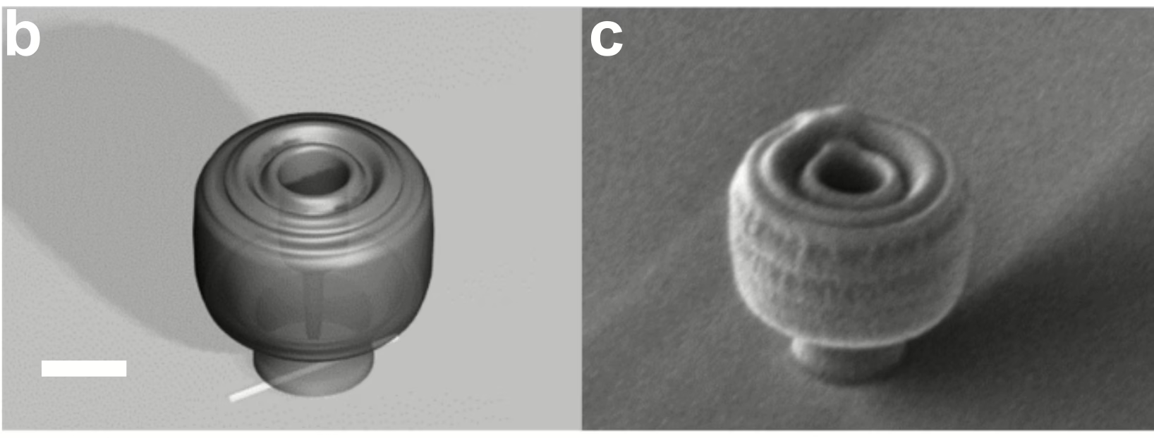
To demonstrate the feasibility of these structures, a proof of concept device was experimentally fabricated. This device involved printing a nanolens structure on top of a gallium arsenide nanowire using a femtosecond pulsed laser technique. Such GaAs nanowires were used for their relevance in photovoltaic devices, while also providing a convenient test system due to their high quantum efficiency (number of photons out per photon in).
Understanding the observed performance
While the nanolenses dramatically improved the directivity of the nanowire emitters, the observed performance was still less than the computational design had predicted. However, by including a small offset between the center of emission and center of the lens, new simulations were able to reproduce the observed behavior. This offset likely occurred in the experimental samples, as the nanowires emit primary from a small region near one of their ends (corresponding the position of the internal diode junction in the wire). The difficulty to align to this emitting location proved to be the single greatest limitation in the observed performance, followed by the fact that this emission was still from a finite region (not a single point, as assumed in the design simulations). This indicates that moving to more confined emitter or absorber structures could easily address both of these sources of decreased performance, and offer even more directive behavior without needing to change the lens or fabrication techniques.

Nanophotonic lens optimization and structure.
(a) Progression of the evolutionary algorithm at four example generations, with cross-sections of the lens structure and the corresponding directivity, D, values shown. The full 3D structure of the final nanolens design is rendered in (b), with a scanning electron microscope image of the actual experimental lenses shown in (c).
Reference
Eric Johlin, Sander A. Mann, Sachin Kasture, A. Femius Koenderink & Erik C. Garnett, Broadband highly directive 3D nanophotonic lenses, Nature Communications 9, 4742 (2018), DOI: 10.1038/s41467-018-07104-1