Researchers in the Photonic Materials group have published their latest findings using cathodoluminescence techniques to measure free electrons moving along a metal surface. The paper ‘Angle-resolved cathodoluminescence interferometry of plasmonic and dielectric scatterers’ is published in the journal Nano Letters on September 18th. The technique can be used for more precise measurements that will benefit computer chip production.
Inspiration

Imagine skipping a stone across a calm pond. Each time the stone hits the water, it creates a wave that spreads outwards. As those waves overlap, they interfere, sometimes amplifying each other, sometimes cancelling out. They create a beautiful, complex pattern on the water.
First author Evelijn Akerboom: “In our recent work, we recreate this phenomenon, but a million times smaller using, electrons and light.”
Cathodoluminescence technique
“We use a technique called cathodoluminescence: where light is emitted when a material is struck by an electron inside the scanning electron microscope (SEM). While SEMs are traditionally used to image very small objects, cathodoluminescence allows us to study how these objects interact with light with a high resolution.”
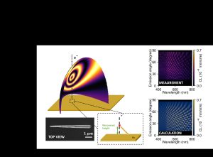
In this project, we investigate cathodoluminescence interferometry where the electron plays the role of the skipping stone. As it flies by a metallic tip, it launches a spherical light wave. A moment later, it interacts with the gold surface below, launching a second wave. Just like ripples on a pond, these light waves meet and interfere. The resulting interference pattern contains valuable information.
What to measure?
Evelijn says: “By carefully analyzing the spacing of the fringes, we measure the distance between two objects very precisely. Also, we can measure how long the electron takes to travel between interaction points. In other words, the time-of-flight of a single electron on the femtosecond timescale.”
Application
While much of this work addresses fundamental questions about electron–light-matter interactions, it also has practical applications. For example, in semiconductor manufacturing, a chip’s quality can suffer from tiny misalignments during fabrication. Evelijn: “Our technique opens new applications for more precise 3D nanoscale measurements during fabrication, helping ensure better chip performance. Turning an i3 into an i7, so to speak.”
To read more details about these findings, read the NanoLetters publication:
Reference
Evelijn Akerboom, Hiroshi Sugimoto, Minoru Fujii, F. Javier García de Abajo, Albert Polman, Angle-Resolved Cathodoluminescence Interferometry of Plasmonic and Dielectric Scatterers, September 18 (2025).
doi.org/10.1021/acs.nanolett.5c02952