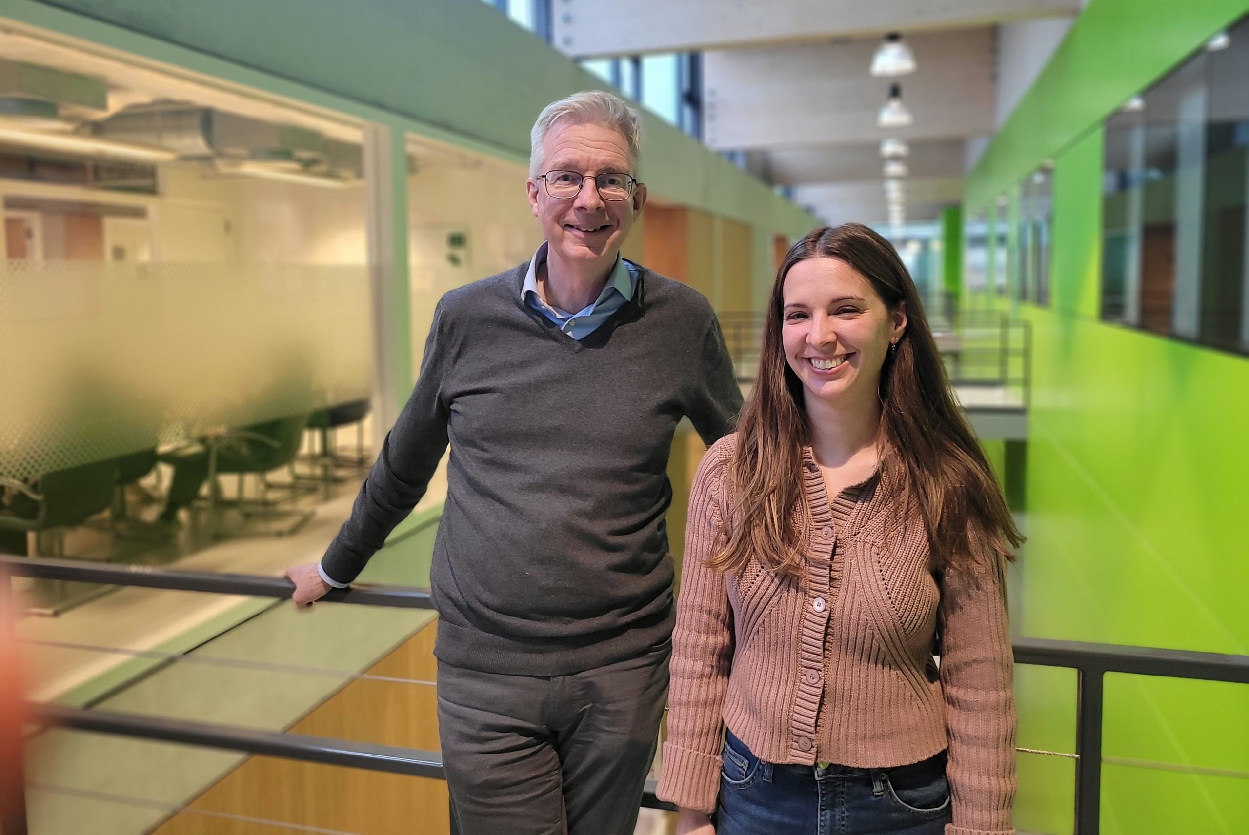
A joint research project between AMOLF, Delft University of Technology, Delmic and Technolution has received funding from the National Growth Fund program ‘NXTGEN Hightech.’ This project, which aims to push the boundaries of microscopy technology, is poised to create innovative tools for semiconductor and life sciences applications. We spoke with group leader Albert Polman and researcher Magda Solà Garcia of AMOLF’s Photonic Materials group, to learn more about this groundbreaking endeavor.
A next-generation microscope
The project focuses on developing an instrument that enables the analysis of large areas with a high (< 5 nm) resolution. Cutting-edge technology, called cathodoluminescence spectroscopy (CL), enables simultaneous measurements with electrons and light. Polman explains: “Typical electron microscopes are limited to smaller samples, but this project seeks to overcome that barrier. For applications in the semiconductor industry, we need to analyze entire wafers, which don’t fit into conventional microscopes. Our approach combines light-electron microscopy with full wafer-scale analysis.”
Collaboration with industry and academia
The collaboration with Delft University of Technology is pivotal to the project’s success. “To analyze larger areas, we’re developing an electron microscope with 64 electron beams,” Magda Solà Garcia explains. Specialists at Delft will design and build the electron column, while AMOLF will focus on the optics to detect light from the sample. “With 64 beams, understanding where the light comes from is a complex challenge,” Polman adds. “AMOLF will build a specialized optical lab to address this complexity.”
The project also involves Delmic, a company co-founded by Polman in 2012. Delmic will provide technical support, with the aim of bringing this instrument to the market. This ensures that the advanced technology reaches industrial users. “This instrument, combining 64 electron beams and integrated optics, is unlike anything that currently exists,” Polman remarked.
Impact on high-tech industry and health research
The potential applications of this new microscope are immense. For the semiconductor industry, it could transform wafer analysis, helping companies like ASML to further improve the quality of their products. “This technology is essential for quality control in computer chip manufacturing, ensuring alignment and defect-free compositions,” Polman noted. The economic impact is equally significant, with high-tech product sales generating substantial returns for the Dutch economy.
The life sciences sector stands to benefit as well. Solà Garcia emphasizes its potential for studying large biological samples. “Some biological samples are often too large for conventional electron microscopes. This new technology allows us to analyze large areas at high resolution, bridging the gap between scale and detail.”
Detail and scale
The project exemplifies the Netherlands’ strength in high-tech equipment development. By merging innovative microscopy techniques with practical industrial applications, it highlights the value of collaboration between research institutes, universities, and industry partners.
“Scale is the central theme,” Polman concludes. “We’re pushing the boundaries to see the smallest details over large areas, a combination that will drive innovation across multiple fields.”
More information
Do you want to learn more about this research project? Then contact Magda Solà Garcia at email address M.Sola@amolf.nl. For more information about AMOLF’s Photonic Materials Group, visit our website.