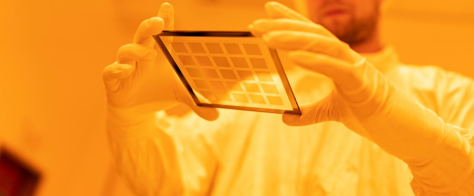
E-beam lithography
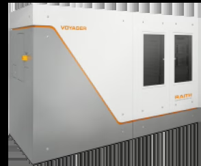
Voyager – Raith
Electron beam lithography system for high-resolution patterning
- Universal sample holder for small sample pieces up to 100mm 10mm max height
- Electron beam energy 10 – 50kV
- Beam current range 50 pA – 40 nA
- Beam size < 2.5 nm diameter at 50 kV
- Minimum feature size 20 nm in high resolution positive resist
- Stage range x=150 by y=150mm z=20 mm
- Mark recognition gives overlay accuracy of <35 nm
- GDSII format viewer and editor
- Import AutoCAD DXF,bitmap, ASCII or CIF format converted to GDSII
- Traxx and Periodixx software option
- FBMS and MBMS software option
AMOLF NanoLab Amsterdam
AMOLF NanoLab Amsterdam is a facility for materials fabrication and characterization down to the nanometer scale. It aims to provide state-of-the art opportunities in nano research, servicing the scientific and engineering community within the greater Amsterdam area.