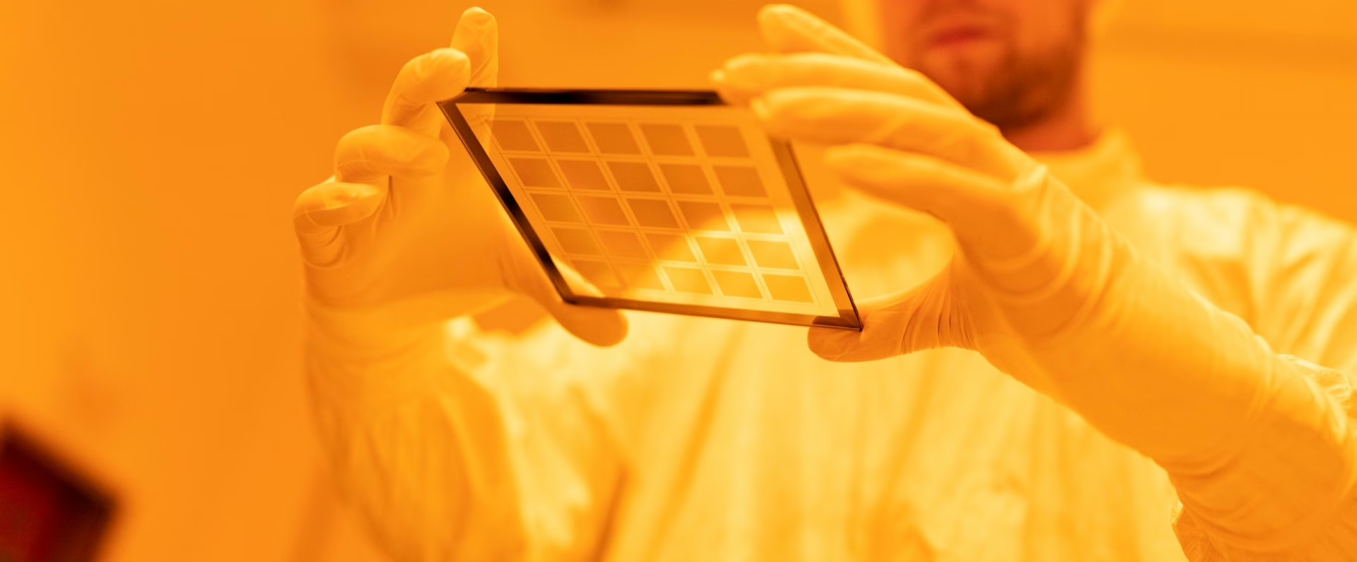
UV lithography
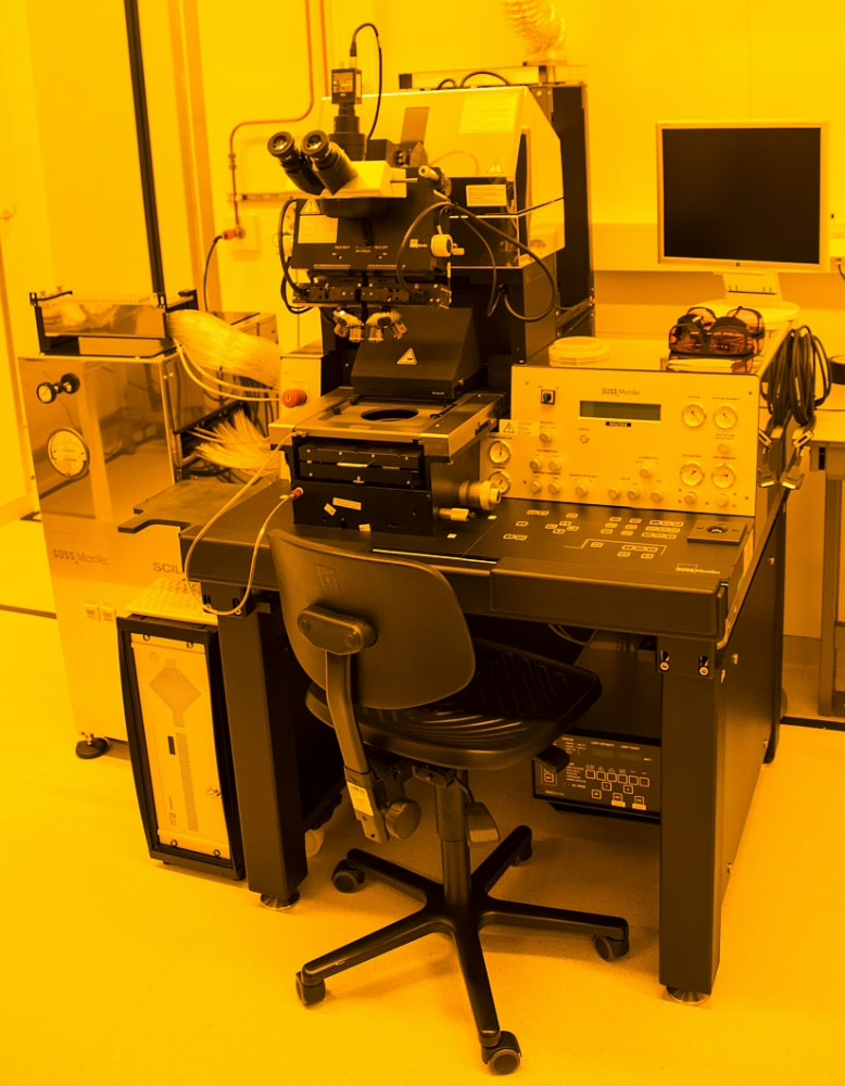
Suss MABA6 UV Mask aligner with SCIL
Optical lithography system. Pattern resolution of sub micron in contact mode.
- exposure lamp Hg 1000W
- normal exposure dose 25 mW/ cm2
- optics wavelength range UV300 280-350 nm (future UV 250 240-260 nm)
- exposure modes; proximity (1-300 mu gap), soft, hard and vacuum contact
- resolution depending on contact mode and mask <1 µm (future 0.5 µm)
- split field topside microscope with 5x, 10x and 20x objective
- bottom side microscope
- bottom and top alignment system accuracy 1 micron
- automatic wedge compensation
- mask holders; opening for 3”, 4”, 6” wafers and 30mm square
- sample chucks; 1”, 3” 4” and 6” wafers
- alignment stage; x +/10 mm Y +/5 mm theta 5°
SCIL (Substrate Conformal Imprint Lithography)
A tool for fabricating nanostructures in which a master pattern is replicated via a stamping process, by molding a liquid material in the inverse shape of the stamp, after which it is solidified. This technique combines the advantages of a soft stamp with a rigid glass carrier for low pattern deformation and best resolution for large area patterning.
- resolution down to sub 50nm on a 6” area
- high aspect ratio structures
- This tool is combined with the UV mask aligner
AMOLF NanoLab Amsterdam
AMOLF NanoLab Amsterdam is a facility for materials fabrication and characterization down to the nanometer scale. It aims to provide state-of-the art opportunities in nano research, servicing the scientific and engineering community within the greater Amsterdam area.