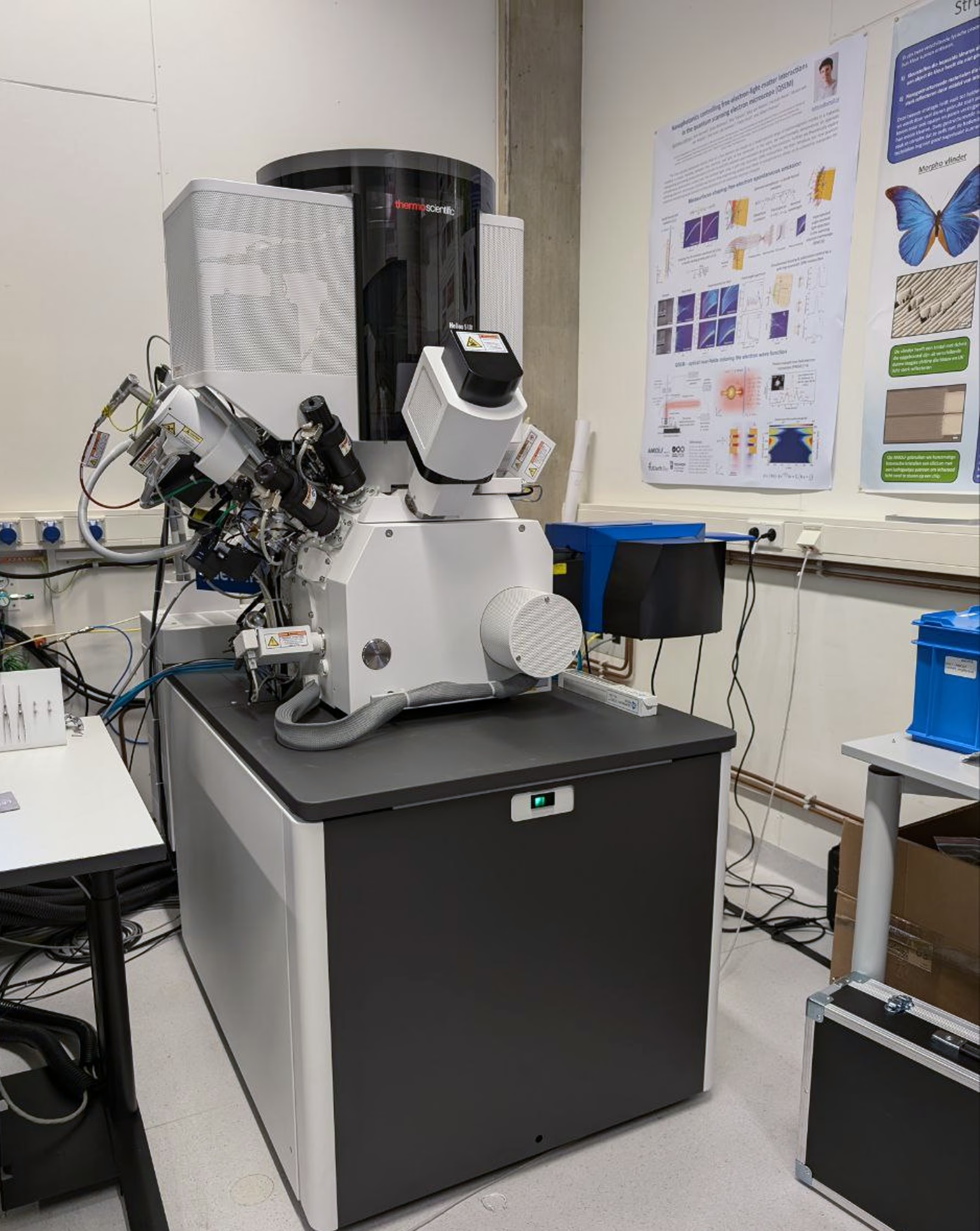
Scanning electron microscope
Thermo Fisher Scienctific Helios UX 5 (Helios 5 UX)
High-resolution imaging with high materials contrast, equipped with EDX, STEM and a SPARC detector for elemental analysis, transmission imaging and cathodoluminescence measurements. It is also equipped with an ultra-fast beam blanker capable of reaching blanking speeds of 50 ns.
This FIB/SEM is equipped with micromanipulators to create TEM lamellae.
- Electron source: Elstar column with Schottky Field Electron Gun (SFEG)
- Electron beam resolution:
- 30 kV in STEM: 0.6 nm
- 15 kV: 0.6 nm
- 1 kV (optimal WD): 0.7 nm
- 1 kV (coincident point): 1.2 nm
- 500 V with ICD detector: 1.0 nm
- Electron beam currents: 0.8 pA to 100 nA
- Electron beam acceleration voltage: 350 V to 30 kV
- Landing energy range: 20 eV to 30 keV
FIB source information
- FIB source: Phoenix column with gallium liquid metal ion source (Ga-LIMS)
- FIB resolution: 2.5 nm to 4.0 nm depending on method
- FIB beam currents: 1pA to 65 nA
- FIB acceleration voltage: 500 V to 30 kV
Detector information
- Elstar in-lens SE/BSE detector (TLD-SE, TLD-BSE)
- Elstar in-column SE/BSE detector (ICD)
- Elstar in-column BSE detector (MD)
- Everhart-Thornley SE detector (ETD)
- IR camera for viewing inside chamber
- In-chamber secondary electron and secondary ion detector (ICE)
- Nav-cam
- Retractable solid-state backscatter electron detector (DBS)
- Retractable STEM 3+ detector with BF/DF/HAADF segments (STEM)
- Integrated beam current measurment
- 60 mm² x-ray detector (EDS, EDX)
Gas-injection system information
- Gas injection systems:
- C
- SiO2
- W
- XeF2
- Base pressure: 2.6×10⁻⁶ mBar
- NanoBuilder software for advanced object design
- AutoScript 4 for Python based scripting
AMOLF NanoLab Amsterdam
AMOLF NanoLab Amsterdam is a facility for materials fabrication and characterization down to the nanometer scale. It aims to provide state-of-the art opportunities in nano research, servicing the scientific and engineering community within the greater Amsterdam area.